
When you look under the hood of generative AI processing, the system design challenges are many. Learn how efficiency, power consumption, and memory issues all come into play.
In less than a year, generative AI saw global fame and use through OpenAI’s ChatGPT, a popular algorithm based on transformers. Transformer-based algorithms can learn complex interactions between different elements of an object such as a sentence or question and transform them into human-like conversational dialogue.
Spearheaded by transformers and other large-language-models (LLM), software algorithms have rapidly progressed, leaving behind the processing hardware tasked to execute them. Even cutting-edge algorithmic processors do not possess the necessary performance to elaborate the latest ChatGPT queries in a timeframe of one or two seconds.
To compensate for the performance inadequacy, leading semiconductor companies build systems made of a large number of their best hardware processors. In doing so, they tradeoff power consumption, bandwidth/latency, and cost. The approach is viable for algorithmic training, not for inference when deployed on edge devices.
Power Consumption Challenges
While training is typically based on fp32 or fp64 floating point arithmetic that generates massive volumes of data, it does not require strict latency. It bears high power consumption and tolerates high cost.
Rather different is the inference process. Inference is typically performed on fp8 arithmetic that still produces large amounts of data, but demands critical latency, low energy consumption, and low cost.
The solution to model training comes from computing farms. Running for days, they use massive electric power that generates lots of heat and costs a fortune to acquire, set up, operate and maintain. Much worse is the inference process, hitting a wall and defeating the proliferation of GenAI on edge devices.
State of the Art in Generative AI Inference at the Edge
A successful hardware accelerator for GenAI Inference must meet five attributes:
- High-processing power in the petaflops range with high efficiency (in excess of 50%)
- Low latency to deliver query’s response in a few seconds
- Constrained energy consumption in 50W/Petaflops or below
- Affordable cost compatible with edge applications
- In-field programmability to accommodate software updates or upgrades to avoid hardware retrofitting with the factory
Most existing hardware accelerators meet some but not all. The venerable CPU is the worst choice because of unacceptable speed of execution; GPUs deliver considerable speed at high power consumption with inadequate latency (thus the choice for training); FPGAs compromise on performance and latency.
The perfect device would be a custom/programmable system on chip (SoC) designed to execute algorithms based on transformers as well as other types of algorithms as they evolve. It ought to support suitable memory capacity to store the massive data embedded in the LLMs and be programmable to accommodate in-field upgrades.
Two obstacles hinder the goal: the memory wall and the high energy consumption in CMOS devices.
The Memory Wall
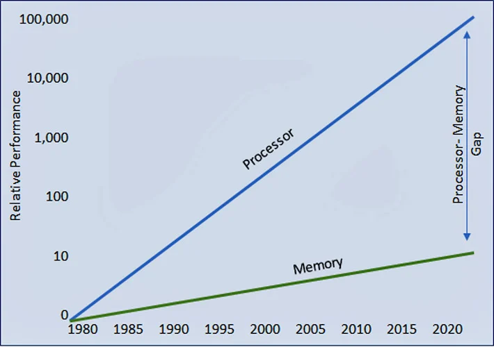
It was observed early in the history of semiconductor development that advancements in processor performance were offset by lack of progress in memory access.
Over time, the gap between the two continued to diverge, forcing the processor to wait longer and longer for the memory to deliver data. The consequence was a drop in processor efficiency from full 100% utilization (Figure 1)..
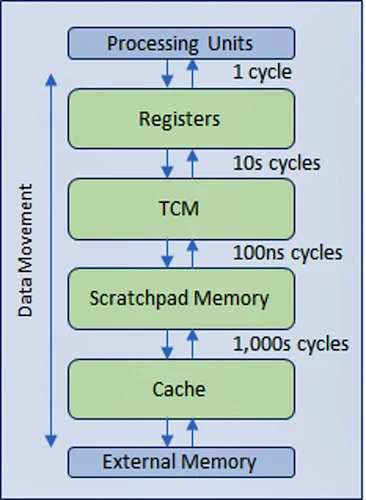
To alleviate the drop in the efficiency, the industry devised a multi-level hierarchical memory structure with faster, more expensive memory technologies nearer the processor for multiple levels of cache that minimize the amount of traffic with the slower main memory and even slower external memories (Figure 2).
Energy Consumption in CMOS ICs
Counterintuitively, power consumption in CMOS ICs is dominated by data movement not data processing. The power consumption of memory access consumes orders of magnitude more energy than basic digital logic computations based on a Stanford University study led by Professor Mark Horowitz (Table 1).
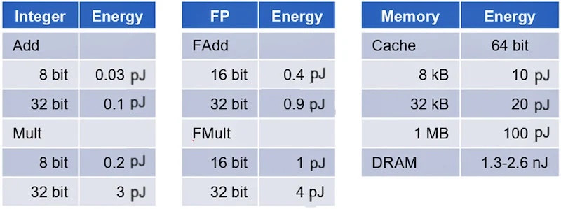
Adders and multipliers dissipate from less than one picojoule when using integer arithmetic to a few picojoules when processing floating point arithmetic. By contrast, the energy spent accessing data in cache jumps one order of magnitude to 20-100 picojoules and up to three orders of magnitude to over 1,000 picojoules when data is accessed in DRAM.
A GenAI accelerator is the quintessential example of design dominated by data movement.
Impact of Memory Wall and Energy Consumption on Latency and Efficiency
The impact of the memory wall and energy consumption in Generative AI processing is becoming unmanageable.
Within a few years, GPT, the foundation model powering ChatGPT, evolved from GPT-2 in 2019 to GPT-3 in 2020 to GPT-3.5 in 2022 to the current GPT-4. Each generation inflated the model size and the number of parameters (weights, tokens and states) by orders of magnitude.
GPT-2 incorporated 1.5 billion parameters, GPT-3 models incorporated 175 billion parameters, and the most recent GPT-4 models pushed the size to approximately 1.7 trillion parameters (no official number has been released).
Not only the sheer volume of these parameters compels memory capacities in the range of terabytes, but accessing them simultaneously at high speed during training/inference pushes memory bandwidth to hundreds of gigabytes/second, if not terabytes/sec. To further exacerbate the scenario, moving them consumes massive energy.
Expensive Hardware Sitting Idle
The daunting data transfer bandwidth between memory and processor and the conspicuous power consumption overwhelms the processor efficiency. Recent analyses show that the efficiency of running GPT-4 on cutting-edge hardware drops to around 3%. The expensive hardware designed to run these algorithms sits idle 97% of the time.
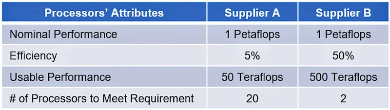
The lower the implementation efficiency, the more hardware is needed to perform the same task. For example, assuming that a requirement of one Petaflops (1,000 Teraflops) may be served by two suppliers. The suppliers (A and B) deliver different processing efficiencies, 5% and 50% respectively (Table 2).
Then supplier A could only provide 50 Teraflops of effective, not theoretical processing power. Supplier B would provide 500 Teraflops of the same. To deliver one petaflop of effective compute power, supplier A would require 20 processors, but supplier B only 2 units.
In one example, a Silicon Valley startup plans to use 22,000 Nvidia H100 GPUs in its supercomputer data center. A rough calculation prices 22,000 H100 GPUs at $800 million—the bulk of its latest funding. The figure doesn’t include the cost of the rest of the infrastructure, real estate, energy costs and all the other factors in the total cost of ownership (TCO) for on-premises hardware.
Impact of System Complexity on Latency and Efficiency
Another example, based on the current state-of-the-art accelerator for GenAI training, will help to illustrate the concern.The Silicon Valley startup’s configuration for GPT-4 would require the 22,000 copies of Nvidia H100 GPUs to be deployed in octets on the HGX H100 or DGX H100 systems, yielding a total of 2,750 systems.
Considering that GPT-4 includes 96 decoders, mapping them over multiple chips may mitigate the impact on latency. Since the GPT structure allows for sequential processing, assigning one decoder per chip for a total of 96 chips could be a reasonable set up.
The configuration translates to 12x HGX/DGX H100 systems that challenge not only the latency due to moving data between single chips, but also between boards and between systems. Using incremental transformers can significantly reduce processing complexity, but it requires the handling and storage of states, which in turn increases the amount of data to be handled.
The bottom line is that the previously mentioned 3% implementation efficiency is unrealistic. When adding the impact of the system implementation with the associated longer latencies, the actual efficiency in real applications would drop significantly.
Put into perspective, the amount of data required for GPT-3.5 is nowhere near that of GPT-4. From a commercial perspective using GPT-3-like complexity is considerably more attractive than GPT-4. The flipside is that GPT-4 is more accurate, making it the preferred choice if the hardware challenge can be solved.
Best-Guess Cost Analysis
Let’s focus on the implementation cost of a system capable of handling a very large number of queries, such as Google-like volumes of 100,000 queries/second.
Using the current state-of-the-art hardware, it is reasonable to assume that the total cost of ownership, inclusive of acquisition cost, operating and maintaining the system, falls in the ballpark of $1 trillion. For the record, that’s about half of the 2021 gross domestic product (GDP) of Italy, the eighth largest economy in the world.
The impact on cost per query of ChatGPT makes it commercially challenging. Morgan Stanley estimated that Google search queries in 2022 (3.3 trillion queries) cost ¢0.2 per query, considered the benchmark. The same analysis stated that the cost per query on ChatGPT-3 ranged between ¢3 and ¢14 per query, 15-70x larger than the benchmark.
The Hunt for Chip Architecture Solutions
The semiconductor industry is feverishly working to find solutions to the cost/query challenge. While all attempts are welcome, the solution must come from a novel chip architecture that will break up the memory wall and drastically lower power consumption.
Industry Articles are a form of content that allows industry partners to share useful news, messages, and technology with All About Circuits readers in a way editorial content is not well suited to. All Industry Articles are subject to strict editorial guidelines with the intention of offering readers useful news, technical expertise, or stories. The viewpoints and opinions expressed in Industry Articles are those of the partner and not necessarily those of All About Circuits or its writers.