
In general, the largest system-on-chip (SoC) designs in industries such as automotive, artificial intelligence/machine learning (AI/ML), and graphics/computing/storage share complexity and size, measured in billions of transistors. They also reveal a multitude of common functional blocks duplicated several times, including central processing units (CPUs), graphic processing units (GPUs), digital signal processing units (DSPs), arithmetic logic units (ALUs), memory blocks, and standard protocol interfaces. Specific functionality required by end-use applications is mostly implemented in software and sometimes via limited specialized hardware.
That is not the case for 5G infrastructure designs and soon 6G designs. While 5G SoCs include common processing units such as CPUs, DSPs and AI/ALUs, most of the fabric is made of sizeable, complex algorithmic blocks implementing a robust set of unique and not repeatable communication functions. They also combine digital blocks with unusually large analog blocks. Furthermore, they employ software to customize their deployment with service providers globally to comply with different standards.
5G wireless communications challenges
The 5G standard became necessary to support ubiquitous, worldwide wireless communications beyond user-to-user communication that drove all preceding standards: 2G, 3G, 4G and a few intermediate versions. The need was dictated as a way to serve the broadest range of user-to-machine and machine-to-machine types of wireless communications including Internet of things (IoT) devices, autonomous vehicles/drones, industrial, medical, military robots, cloud-based AI/ML services, edge applications, and more.
Expectedly, the dramatic expansion in applications produced an explosion of data traffic, particularly in urban areas. Figure 1 compares the growth in Exabytes from 2010 to 2030.
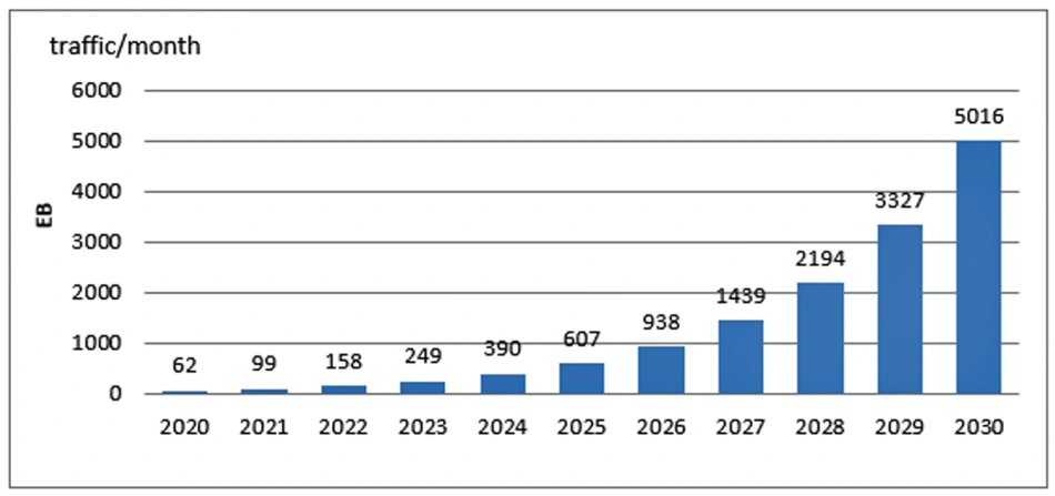
Figure 1 Dramatic expansion in applications produces an explosion of data traffic in Exabytes from 2010 to 2030. Source: International Telecommunications Union-Radio Communication Sector (ITU) Report ITU-R M.2370-0
The combination of escalating data traffic with faster data communication compounded with significant shorter latency led to the perfect storm in the form of challenges never seen in the wireless technologies before.
Among the challenges, 5G bandwidth increased more than 20-fold to more than 20 gigabits per second, speed expanded from a few gigahertz to hundreds, latency dropped from tens of milliseconds (ms) to 1 ms, and the number of concurrent users jumped by orders of magnitude. All combined, the extreme attributes called for upgrading the existing communications technologies, and to a larger extent, for new design verification/validation tools and methodologies.
To address the dauting specifications, the industry devised a series of new technologies. Among the most relevant are:
- Millimeter waves to support many simultaneous high-bandwidth channels each transmitting and receiving immense amounts of data, and to reduce or eliminate the lag in wireless video calls or fast responses in driverless vehicles to avert accidents
- Beamforming to optimize transmission power and increase network capacity
- Massive multiple-input-multiple-output (mMIMO) radio to increase the efficiency of a network while reducing transmission errors
- Carrier aggregation to augment the efficiency of a communication
- Small cells to create a denser infrastructure to ensure broad and consistent service
The long list of features and capabilities encapsulated in the 5G standard imposed the redesign from the ground up of the 5G infrastructure implemented in the base station unit (BBU). Figure 2 portrays nine major challenges that the 5G infrastructure had to address.
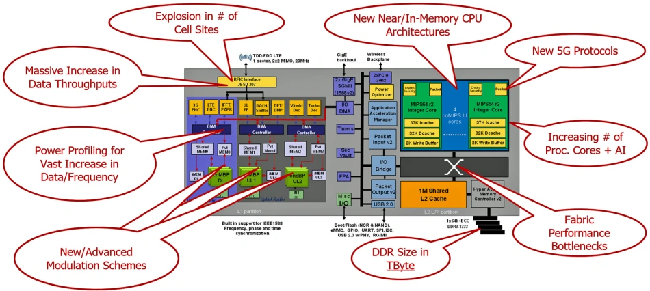
Figure 2 Nine main issues hinder the development of the 5G infrastructure. Source: Marvell Technology
Brief description of 5G base station
To size the 5G BBU development task, one can peek into any literature describing a 5G base station. While in all previous wireless generations, the BBU consisted of two monolithic blocks—core network (CN) and radio access network (RAN)—the 5G BBU needs an acronym soup of functional blocks to be described.
First off, the architects “disaggregated” hardware and software in three main blocks: front-haul (FH), mid-haul (MH) and back-haul (BH). Then, they moved sections of the core network of older wireless generations into the FH and split the FH in the central unit (CU), distributed Units (DU) plus several Radio Units (RU), now served by arrays of antennas (see Figure 3).
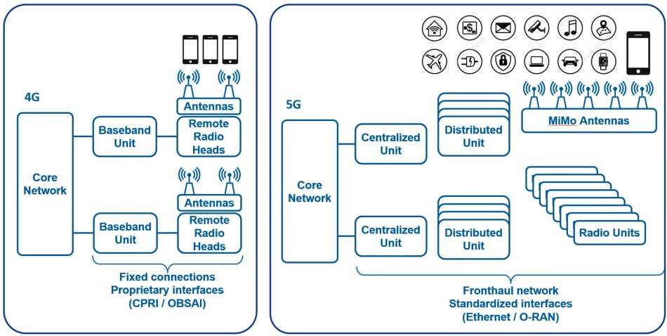
Figure 3 A 4G base station diagram looks different than the 5G BBU, a completely new design. Source: Siemens EDA
The disaggregated 5G Central-RAN (C-RAN) allows for installing CUs, DUs, and RUs remotely from each other, leading to several advantages:
- Decentralized units provide a cloud-based RAN that covers a much larger area around cities than the BUs used by 4G networks.
- 5G RU can drive up to 64×64 MIMO antennas that can support beamforming and achieve massive increase in bandwidth at significantly lower latency.
- Multiple DUs work together to dynamically allocate resources to RUs based on network conditions.
- The wireless RU network connects wireless devices similar to access points or towers.
Other benefits of the C-RAN network embrace the ability to flexibly pool resources, reuse infrastructure, simplify network operations and management, and support multiple technologies. They lower energy consumption, avoid rebuilding the transport network, shrink capital and operational expenses, and dramatically reduce total cost of ownership (TCO)
Because the 5G network structure is more heterogeneous and self-organizing, it’s easier to evolve to meet changing market conditions and new opportunities. A 5G network can be customized as needed in cities and rural areas, leading to new hardware/software configurations and use cases available to cellular operators.
Architecting the 5G BBU presented the opportunity to break the traditional monopoly, benefiting a few wireless providers and open the market to 5G BBU developers. Today, any wireless design house can develop any 5G BBU components as long as they comply with interface protocols.
To this end, a large alliance of telecommunication industry members sponsored the open radio access network (O-RAN) standard, an open standard defined by the O-RAN Alliance. The goal of the standard is to utilize the same physical cables used within an Ethernet network.
5G wireless BBU verification challenges
The complexity of the architecture is rooted in the requirement to support a broad range of wireless functionality and several different types of use cases like centimeter waves, millimeter waves and dynamic changes such as carrier configurations, among others. Not to mention, compatibility with all previous wireless standards.
The entire base station is physically constrained to a single PCB populated with a few large SoC devices in either 7-nm or 5-nm process technology. These sizes are in the ballpark of the largest silicon chips found today in the semiconductor industry.
The multiple BBU chips must be verified in isolation from one another; it’s critical because some of the chips are sourced from different design houses. Non-standard interfaces between sections of a design and between chips at the full system level hinder stimulus generation. The scenario must be verified for more than 10 ms of real time, a long stretch for verification, impacting the bottom-up or divide-and-conquer approach, thwarting exhaustive verification and ruling out accurate gate-level simulation for lacking the necessary performance.
Vis-à-vis such a demanding load, the allocated time for debugging falls in the ballpark of one or two weeks. Recent focus on energy efficiency and security issues intensifies the verification efforts, pushing it to new limits.
Since the lifespan of 5G infrastructure products ranges from 10 to 15 years, design verification does not stop after pre-silicon and post-silicon are fully validated, or even when products are delivered. It is not uncommon to get requests for customer support several years after the product was shipped. For example, a request to debug some new software features when the original development team has been reassigned to new tasks.
Dr. Lauro Rizzatti is a verification consultant and industry expert on hardware emulation.
Author’s Note:
Special thanks to Dr. Ashish Darbari, CEO of Axiomise; Anil Deshpande, associate director at Samsung Semiconductor India; Axel Jahnke, Nokia’s SoC R&D manager; Oren Katzir Real Intent’s vice president of applications engineering; and Herbert Taucher, head of research group at Siemens AG. They participated in “5G Chip Design Challenges and their Impact on Verification,” a DVCon Europe 2022 panel moderated by Gabriele Pulini, product marketing and market development at Siemens EDA. Each graciously took the time to talk with me after the panel to offer more insight into the challenges of 5G chip design and verification.