
In this column, we review the state-of-the-art in solid state drives (SSDs) and propose a methodology for the verification and validation of the SSD controller
Source: EE Times
Note: This is the third in a series of articles on digital data storage. In Part 1, Digital Data Storage is Undergoing Mind-Boggling Growth, we considered the evolution of digital data. In Part 2, Data Storage: The Hard Disk Drive, Ben Whitehead, Mentor Graphics’ storage product specialist, covered the hard disk drive (HDD), discussing its technology and the verification challenges that pave the way for testing its design. Now, in Part 3, I review the state-of-the-art in solid state drives (SSDs) and propose a methodology for the verification and validation of the SSD controller, which is the most critical part of an SSD drive design.
An SSD stores data on semiconductor fabric. Currently, the most popular technology for SSDs is NAND Flash, a non-volatile memory (NVM) component. Based on a single transistor per bit of data, NAND comes in a few variations as follows:
- The single layer cell (SLC)
- The multi-level cell (MLC)
- The triple-level cell (TLC)
NAND Flash can include more than three levels, but with additional levels the data access slows and reliability is compromised.
Today, NAND Flash dominates the SSD landscape, with forecasted growth expected to go from 100 Exabytes (EB) in 2016 to 750 EB in 2020. The SSD business includes five companies manufacturing NAND Flash memories, such as Samsung, SK Hynix and Micron; 19 companies developing SSD application specific integrated circuit (ASIC) controllers; and more than 160 companies integrating the controllers in SSD devices.
Unlike the HDD business, the barrier to entry for a new SSD business consists of assembling all the parts and selling a complete product. Third-party integrators buy off-the-shelf components; i.e., they purchase a controller from one of the 19 companies developing them and combine this withFlash from one of the big five. They then develop software or firmware on top, encapsulate the whole into a package, and sell it as a finished storage device.
SSD Technology
An SSD has no moving mechanical parts, a fundamental difference from the traditional electromechanical storage paradigm. Instead, an array of NAND Flash memory cells makes up the storage media. Lacking any spinning mechanical parts, the SSD operates much faster than traditional HDD devices, and is virtually free of the data access latencies present in electromechanical storage devices. Additionally, solid-state storage consumes less power, produces less heat, and runs quietly with no vibrations during operation. SSDs are more resistant to physical shock, and data is not erased by proximity to magnetic sources. All combined, these characteristics contribute to their significantly higher reliability than HDDs. The typical mean-time-between-failure (MTBF) of an HDD hovers at around one-million hours, compared to well over two-million hours for an SSD.
There are, however, a few downsides to SSD technology. Although there are no moving parts inside an SSD, each memory cell has a finite life expectancy — namely, a limit on the number of times it can be written to and read from before it stops working. This is due to the physics of the writing/erasing mechanism of the semiconductor cells.1 Logic and firmware built into the drives dynamically manage the SSD operations to minimize problems and extend their life.
1The programming process for a Flash cell requires the use of high voltage to charge/discharge the floating-gate transistor sandwiched between the control-gate transistor and an oxide layer. Charging the floating gate is referred to as programming the cell and equates to a logic “0.” Discharging it is referred to as erasing the cell and equates to a logic “1.” Over time, the charging/discharging or erasing/programming cycles via high voltage stresses the oxide layer, and shortens the cell life. This leads to a finite number of erase/write cycles of the NAND Flash.
Further, SSD devices have higher per-gigabyte prices than electromechanical storage devices and generally support smaller capacities.
Data stored on a NAND Flash fabric is organized in a hierarchical structure. From the bottom up, the memory cells are organized in strings, pages, and blocks. Strings are typically comprised of 32- or 64-NAND cells and provide the minimum readable units. Multiple strings make up a page, which typically includes 64K or 128K cells, referred to as 2 kilobytes (Kbytes), 4KBytes, 8KBytes, etc. Pages are the minimum programmable units, and multiple pages form a block, which is the minimum erasable unit. Currently, the maximum pages per block are approaching 512 and block sizes are reaching 8 megabytes.
SSD devices possess a few characteristics that set them apart from HDD devices. Among the most important are write amplification, wear leveling, garbage collection, and performance degradation over time. Other issues such as overprovisioning and Self-Monitoring, Analysis, and Reporting Technology (SMART) add complexity to the drive.
Write Amplification: In an SSD, NAND Flash cells must be erased before they can be rewritten again. The net result is that data is rewritten multiple times, thereby increasing the number of program/erase cycles over the life of the device. This leads to a write amplification issue that decreases the lifespan of the device and impacts performance.
Wear Leveling: Unlike in an HDD where data can be written over and over in the same location on the disk surface without causing any problem, new data is written in an SSD to different NAND cells for the purpose of wear leveling. The physics overlooking the programming mechanism of a NAND cell impose erasing the cell prior to writing new data. Since the smallest erasing unit is a block, typically made up of 32 to 64 pages, erasing a block is time consuming. Due to the limited number of erase/write cycles inherent to the technology, called endurance, erasing/writing a block repeatedly without involving other blocks would wear out that block before all other blocks, prematurely ending the life of the SSD. To avoid the catastrophic event, SSD controllers use a technique called wear leveling that distributes writes as evenly as possible across all blocks in the SSD. The technique is based on complex algorithms implemented in firmware that require exhaustive testing in the development stage.
Garbage Collection: Another difference between an HDD and an SSD concerns the deleting of a file on the host computer.
In an HDD, deleting a file in the OS running on the host leaves bits on the hard drive. Since writing a file on empty blocks in an SSD is faster than on a written block, a TRIM feature automatically deletes the entire file’s data as soon as the file is deleted in the OS running on the host. As the SSD fills up, fewer and fewer empty blocks become available. In their place are partially filled blocks. The SSD cannot write the new data onto these partially filled blocks since it would erase the existing data. Instead, the SSD reads the data of the block into its cache, modifies the old data with the new, and then writes it back.
Garbage Collection is the process of reclaiming previously written blocks of data so they can be rewritten with new data. Garbage Collection is implemented in algorithms mapped in firmware in the SSD controller and critical to the SSD’s operations.
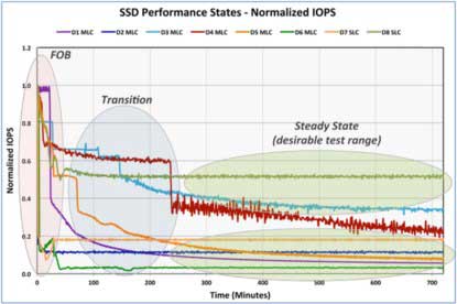
Performance Degradation: In a brand new SSD device, all NAND Flash cells have never been written, and their floating-gate transistors have never been charged. In other words, they include logic “1s.” When deployed, the erase/write process begins. At this stage, the performance measured in input/out operations per second (IOPS) exhibits its maximum value.
As the workload increases, the SSD controller is forced into an erase/write cycle for every pending write operation. Due to this process, the SSD performance gradually drops until it finally settles into a steady state. The chart shown in Figure 1 shows the degradation curves for eight types of SSD devices. IOPS (input/output operations per second) in a steady state is typically less than 50% and as low as 5% of its maximum value when the device is new.
SSD Controller
The conceptual simplicity of the NAND Flash fabric belies the complexity of the SSD operations. The burden to manage the SSD’s uniqueness and peculiarities falls on the SSD controller.
Figure 2 represents the block diagram of an SSD controller. It encompasses six sections: host controller interface; controller System-on-Chip (SoC); NAND Array; DDR RAM for caching both user data and internal SSD metadata; and, the most critical component, system firmware stored in large SRAMs, plus a NOR Flash.
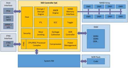
Figure 2. The SSD controller includes host controller interface, controller SoC, NAND Array, DDR RAM, system firmware, and NOR Flash(Click here to see a larger image. Source: Mentor Graphics)
Host interface: The host interface of an SSD controller typically is based on one of the industry standard interface specifications, the most popular being SATA/SAS and PCIe. Since the host interface is the performance bottleneck, the preferred standard is PCIe. An emerging standard called Non-Volatile Memory express (NVMe), using PCIe as the fabric, provides the fastest performance.
Controller SOC: The Controller SoC is built around a CPU/RISC processor complex that may include multiple processors. All the processors communicate with each other but perform different tasks, such as managing the PCI traffic, read and write caching, encryption, error correction, wear leveling, and garbage collection, to name a few.
Firmware: The firmware is the most complex part of the controller. The embedded microcode manages all the operations that set the SSD apart from the traditional HDD. It implements the algorithms that perform the Garbage Collection, the wear leveling and several other tasks. If not properly designed, the algorithms may affect efficiency, reliability and performance of the SSD. A major cause of data loss in SSDs is due to firmware bugs.2
2The firmware is a challenge faced by third-party integrators. Attracted by the growing business opportunities, they purchase a few off-the-shelf components, assemble them on a PCB, add firmware and assume the drive is ready to be sold, only to discover that the controller does not work as expected or not at all.
Vis-à-vis the complexity of the firmware, the SSD hardware is not particularly large when compared with designs in other market segments like networking or processor/graphics. An enterprise-level controller design with loads of functionality implemented in hardware may reach a capacity of 60-100 million gates. Meanwhile, a client-level controller in which most of the functionality is realized in firmware may have a gate count of 20 million.
SSD Controller Design Trends
SSD technology is on the move as the firmware continues to grow and implement more and more functionality. So too is the NAND array in size and in number of instances.
The speed of the interface between the NAND array and the controller SoC is faster than the host interface and continues to increase, enlarging the performance gap between the two.
The overall complexity and size of the controller SoC also expands to cope with the increasing complexity of the NAND management.
As with all modern SoC designs, reducing power consumption is a critical requirement, and this trend will continue.
Design and Verification of an SSD Controller
The uniqueness of the SSD controller design is amplified by its verification/validation process. Unlike most chips in mobile designs that may be built on commercial intellectual property (IP) or run on a standard Linux kernel, the SSD controller must be designed from scratch. The hardware and embedded firmware must be highly customized and closely coupled. The hardware may use a few standard IP blocks such as CPUs, system buses, and peripherals like UARTs, but the firmware determines the major features of the SSD controller. To achieve the best performance and the lowest power consumption, the firmware must be fine-tuned on optimized hardware.
To accomplish this, the industry is adopting a software-driven chip design flow, as opposed to the traditional hardware/software design flow.
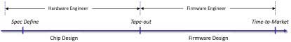
In a traditional hardware/software design flow (Figure 3), hardware and firmware designs are serialized or pipelined. Firmware engineers may participate in the system definition specs, but firmware implementation details are deferred to post tape-out when the hardware is completed. This flow leads to poor firmware functionality and limited performance. Also, since firmware development starts late, the design cycle increases considerably, oftentimes leading to missed schedule deadlines.
By comparison, in a software-driven design flow (Figure 4), firmware development starts at the same time as the hardware design. Firmware engineers participate in the spec definitions of the hardware and gain intimate knowledge of the hardware details during the hardware design phase. Since the development of hardware and software proceeds in parallel, they can influence each other. Testing early firmware on the hardware in development unearths bugs that otherwise would be found after tape-out. Likewise, performance optimization can occur early on.
By the time the design is ready for tape-out, hardware and firmware have been optimized and are virtually ready for mass production. When engineering samples are returned from the foundry, the lab bring up of hardware and firmware may require only one or two weeks, thereby dramatically accelerating time to market compared to the traditional design flow.
The design verification/validation in a software-driven design flow necessitates a high-performance system as close to the real chip environment as possible with powerful debug capabilities and easy bring up.
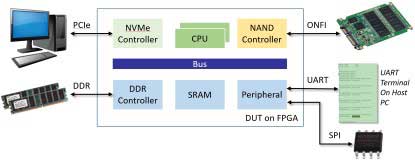
A traditional field programmable gate array (FPGA)-based prototyping board, as depicted in Figure 5, meets some of the requirements, such as speed of execution, but it also brings along a few drawbacks.
This setup involves the deployment of physical peripherals: an array of NAND Flash devices connects to the NAND controller mapped inside the FPGA and a set of DDR memory connect to the DDR controller in the FPGA. Peripheral interfaces, like UART and SPI, and a physical PCIe or NVMe interface to the host complete the setup. While an FPGA board is close to the real hardware, and supports the high-speed execution necessary for firmware validation, several disadvantages affect its deployment.
For example, the complier supports only a synthesizable subset of the register transfer level (RTL) language and models often need to be rewritten to fit the structure of the FPGAs. The bring up of the real peripheral devices imposes substantial effort to cope with electrical, mechanical, power dissipation, frequency modulation (FM) interference, and noise issues. Design debug in an FPGA is hard and time-consuming due to the poor internal design visibility created via compilation. Adding visibility forces recompilation of the whole design, thereby slowing down the entire verification process.
Fortuitously, hardware emulation solves all of these difficulties. A modern emulator possesses several advantages over an FPGA-based prototype. Mapping the design RTL code onto the emulator requires limited code modification. The emulator offers full design visibility similar to a hardware description language (HDL) simulator, but at four to five orders of magnitude faster speed, closer to that of the FPGA prototype board, which is mandatory for firmware development. Such an emulator becomes a shared resource, accessible remotely if deployed in virtual mode, which is not possible with FPGA-based prototypes.
Emulators can be deployed in in-circuit-emulation (ICE) or virtual mode. The ICE mode follows the same path as the FPGA-based prototyping approach, and suffers from the same problems introduced by the physical peripherals. The virtual mode resolves all of the issues, preserving the benefits of an emulator.
In a virtual setup, all peripherals are modeled in software giving engineers full control and visibility of the emulation environments, not just the design under test (DUT), but also of peripherals and interfaces (Figure 6).
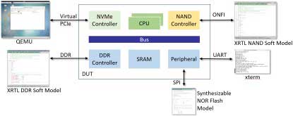
Figure 6. In a virtual setup, engineers control the emulation environment (Click here to see a larger image. Source: Lauro Rizzatti)
Soft models implement the NAND Flash and DDR memory running on the emulator or host server. A serial peripheral interface (SPI) NOR Flash model can be synthesized and executed on the emulator. The PC server, connected to the DUT inside the emulator via a virtual PCIe based on a DPI interface, hosts a Quick EMUlator (QUMU) virtualizer. A UART model connects to an xterm window running on the host server. All virtual models are controllable and visible on a single host server connected to the emulator.
The virtual solution affords several advantages. First, it permits full-signal visibility of the DUT and the external virtual devices and their interfaces. PCI traffic can be monitored. The host OS runs a QEMU virtualizer providing complete control of the behavior of the BIOS. The contents of the DDR memory, NAND Flash, and SPI NOR Flash can be read and written. Their types and sizes can be many different configurations, which is an impossible feat in a physical setup. The virtual domain offers a convenient debugging environment because everything can be seen and modified.
In the case of the PCIe interface, for example, VirtuaLAB PCIe from Mentor supports thorough debugging of the interface and monitoring of the traffic via a built-in virtual PCIe analyzer.
The virtual setup adds three capabilities not viable with a physical setup as follows:
- It can be accessible remotely 24/7 from anywhere in the world.
- It can be shared by a multitude of concurrent users.
- It supports the same clock frequencies as the actual design since the peripheral clock frequencies do not have to be slowed down via speed adapters to match the slow-running clock of the emulator. This avoids discrepancies from different speed ratios and enables realistic performance evaluations.
The virtual emulation environment is identical to the real-chip environment after the chip is released by the foundry. It can test the firmware, check design performance, and find bugs that cannot be found via an HDL simulator, and it facilitates architectural experimentation to accommodate different media storage types and interfaces.
Conclusions
To take advantage of the escalating market growth of SSD devices, engineers must accelerate the development cycle and avoid the risk of delivering under-tested and low-performing chips.
Only a state-of-the-art emulation platform can accomplish this demanding mission. Via its fast execution speed comparable to an FPGA prototyping board, and a fast and straightforward setup, an emulator deployed in virtual mode provides a suite of debugging capabilities that become the centerpiece of a software-driven design flow.
The SSD industry has proven it is possible to shed two to four months off the development cycle with emulation. When combined with deployment as a shared and remotely accessible resource, the return on investment (ROI) of an emulation system can certainly be justified.
Dr. Lauro Rizzatti is a verification consultant and industry expert on hardware emulation (www.rizzatti.com). Previously, Dr. Rizzatti held positions in management, product marketing, technical marketing, and engineering. He can be reached at lauro@rizzatti.com.