
My head is currently spinning like a top. I foolishly wondered how much power AI-heavy data centers are currently consuming, and how much they are expected to consume in the coming years, and now I’m sorry I asked.
The International Energy Agency (IEA) forecasts that global electricity demand from data centers will more than double to approximately 945 TWh by 2030, primarily driven by AI-optimized facilities. That’s about the current annual electricity use of Japan. A Deloitte estimate predicts that worldwide AI data center consumption will reach ~90 TWh by 2026, which would account for roughly one-seventh of all data center power use (681 TWh).
By 2030, US data centers are expected to consume approximately 8% of the nation’s electricity, up from 3% in 2022. Utility delays for data center grid connections can stretch up to seven years. Without upgrades, AI expansion could outpace the electric grid’s ability to keep up.
According to Data Center Dynamics, Google CEO Sundar Pichai has stated that the company is now designing data centers that require over 1 gigawatt of power, which is roughly equivalent to the entire output of a conventional large nuclear reactor.
Fortunately, the use of AI is slowing down and is expected to decline next year.
I’M JOKING! (You’re so easy.) In a 2024 forecast, Gartner said that AI inferencing compute demand is expected to grow at a ~40–50% compound annual growth rate (CAGR) through 2027, much faster than most other datacenter workloads. Also in 2024, the International Data Corporation (IDC) estimated that by 2028, ~80–90% of all AI compute in the cloud will be inference, not training, since once models are trained, they’re deployed and queried billions of times. In a crunchy nutshell, total AI inference compute demand is projected to increase by an order of magnitude over the next five years.
Suppose you are the proud owner of an AI data center (or that you are in the process of building one). Now, suppose I told you I knew a way to halve the amount of power required to perform AI inferencing on large language models (LLMs). Of course, knowing the ways of the world, what you’d probably do would be double the amount of inferencing you were performing while maintaining the same power envelope, but that’s just a different way of looking at the same thing.
The reason for my waffling about all this here is that I was just chatting with Jan Pantzar, who is VP of Sales and Marketing at VSORA. This is a French fabless semiconductor company, founded in 2015 by a team of seasoned DSP and AI engineers, based in Meudon-La-Forêt near Paris, with additional offices across Taiwan, Japan, Korea, and the US. Their mission is to deliver ultra-efficient, high-performance chips designed specifically for real-time inference—not training—with a focus on reducing latency, lowering power consumption, and cutting the cost per query
The last time Jan and I spoke was circa 2020/2021. At that time, VSORA had recently released an intellectual property (IP) block for other designers to incorporate into their System-on-Chip (SoC) devices. The primary target market at that time was the automotive industry.
This IP provided a combination of AI inferencing and DSP. It also provided 1 petaflop of inferencing power, which was around eight times the performance of anything else available on the market at that time. In fact, this little scamp received the “Best Processor IP of the Year” award from the Linley Group (now part of TechInsights).
The way in which (and the reasons why) the guys and gals at VSORA transmogrified themselves from an IP provider into a fabless semiconductor company is jolly interesting, but not particularly relevant to the tale I’m about to tell. All we really need to know is that they’ve designed an AI chiplet that provides sufficient inference performance to make your eyes water while also being 4 to 5 times more efficient than anything else on the market.
Take a look at the image below. This shows the insides of VSORA’s flagship product, the Jotunn 8. Implemented using TSMC’s 5nm technology node and intended for AI data center inferencing, this bodacious beauty boasts eight of the aforementioned VSORA chiplets along with eight high-bandwidth memory (HBM3E) die stacks. The external host processor can be an ARM, X86, RISC-V, etc.
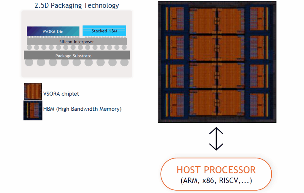
Each VSORA chiplet contains two AI cores (inferencing engines), which account for the bulk of the logic. Furthermore, almost as an aside, each chiplet also contains five RISC-V processors (meaning the Jotunn 8 contains 40 of the little rascals), each measuring less than 1 square millimeter. Two of these RISC-V processors are associated with each AI inferencing engine, while the fifth performs arbitration and other functions.
The idea is that when running an inferencing algorithm, we don’t want to control the algorithmic layers in the inferencing engine from the host processor. Therefore, the host system simply offloads these tasks onto the RISC-V processors in the chiplets and then waits for the results to be returned.
What? You want more details? Well, one reason for having two RISC-V processors per core is functional safety (FuSa). This derives from the team’s original automotive target for its IP cores, allowing the two processors to be put in lockstep if required. Would we ever want to do this in a data center deployment? I have no idea. However, the beauty of chiplets lies in their scalability. For example, the chaps and chapesses at VSORA also offer Tyr devices with 2 or 4 of these chiplets for edge AI inferencing applications, which could take place in automobiles, but we digress….
Returning to the Jotunn 8, this provides an eye-watering 3.2 petaflops of fully programmable processing power. It supports 4-, 8-, 16-, and 32-bit floating-point processing along with 8-, 16-, and 32-bit integer processing. It also offers 288 gigabytes of HBM memory along with 8 terabits-per-second data bandwidth. O-M-Goodness gracious me, is all I can say.
Do you recall my recent column, The Wizard of Oz and Mozart Meet Generative and Agentic AI? In that column, we considered some of the differences between “old and boring” generative AI compared to “new and exciting” agentic AI. The reason I make mention of this here is that Jan notes that, since VSORA’s origin is in the DSP world, the VSORA chiplet’s instruction set is very rich, allowing it to easily handle more complex algorithms than traditional transformer-based LLMs, including the new agentic AL that’s coming into play.
But wait, there’s more! How is it that the VSORA chiplet (and hence any multi-die systems based upon it) is so efficient? The answer is in the architecture. The following is a highly simplified representation, but it gives the idea.
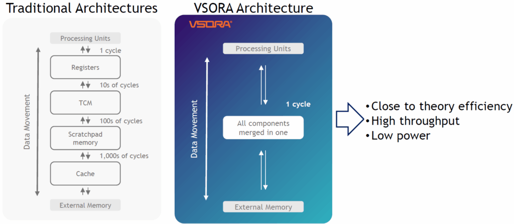
Traditional architectures employ memory hierarchies. The processing units can communicate with registers in just one clock cycle, but the registers are limited in number. Next up is tightly-coupled memory (TCM) and/or scratchpad memory. Next, we have L1 and L2 cache. All of this is on the same silicon die. The term “external” in the above diagram just means “external to the die,” and not necessarily external to the package. This “external” memory could be both in-package HBM and out-of-package DDR. The problem with traditional architectures is that they spend most of their time preparing data for processing, rather than actually processing it.
Now compare this to the VSORA architecture. What the folks at VSORA have done is merge all the traditional memory components into a single unit. We can think of this as 16 million registers for each inferencing engine, so 32 million registers for each chiplet (remember there are two engines on each chiplet), and 256 million registers for each Jotunn 8. Each of these registers can be accessed (read from or written to) by its own inferencing engine in a single clock cycle.
Is this making your head hurt? Imagine what it does to a compiler. In fact, there probably isn’t a compiler around that can handle the 16 million registers on a single inferencing engine, let alone the 256 million registers in a Jotunn 8. Happily, it doesn’t have to; at least, not in the way we usually think about these things, which is as registers having addresses.
Jan explains things as follows: “We don’t handle scalars in the hardware—we handle matrices, vectors, and tensors directly in the hardware. Which means that the moment you load data into the register file, the only thing we handle are indices. And that makes things much easier. Then data is shuffled using streams. So again, there’s no need for any addresses. It’s just indices. And it’s this that gives you the efficiency.”
I bet this sounds easier than it really is, but I didn’t wish to delve deeper because my head was already hurting.
Before we close, Jon Peddie Research’s AI Processor Development report is a supply-side report series that covers the AI processor market size, value, and segment type. The Q3 2025 AI Processors Market Development Reportis available now to JPR subscribers. It includes a companion database that covers over 1,700 data points for every tracked company, along with analyst commentary and quarterly updates.
In this report, 121 companies have been identified as either producing or threatening to produce an AI processor, ranging from small IoT-class devices to hyperscale data center accelerators.
As Dr. Jon Peddie, president of JPR says: “AI processors are experiencing a Cambrian explosion, reminiscent of the 3D graphics boom of the late 1990s and the XR wave of the 2010s. We expect rapid consolidation in the coming years, with the 121 players we track today shrinking to around 25 survivors by the end of this decade.”
We live in exciting times. These times are certainly going to be exciting for the 121 players noted in the Peddie report, but I, for one, have a high level of confidence that VSORA is destined to be one of the 25 survivors. What say you? Do you have any thoughts you’d care to share on any of this?