

Despite abundant rumors predicting the end of life for Moore’s Law (the axiom stating transistor density doubles every 24 months), semiconductor design sizes continue to grow exponentially with no end in sight. In the process, design sizes push costs off the roof.
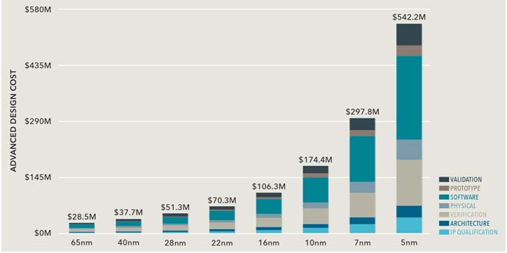
According to market research International Business Strategies (IBS), the total cost of designing a state-of-the-art system on chip (SoC) at the 5nm process technology node exceeds half a billion dollars. Of all the stages that make up the entire design creation and verification flow, two account for more than 60% of the total cost. Hardware design verification consumes about $120M, and embedded software development and validation approximately twice as much, and the trend continues, as shown in Figure 1.
Why such bewildering costs? What tasks and objectives do they accomplish?
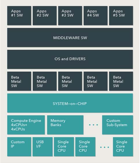
The short answer is design complexity. Over the past two decades, hardware complexity progressively increased exponentially, and so did software code. From a fabric that consisted mostly of single embedded processors, some memory, and large amount of hardwired logic in the form of commercial IP and custom blocks, design structures morphed into a Lego-like multi-layered hierarchy. In parallel, software content amplified in volume and increased software teams to offset hardware teams by several multiples. Hardware and the software structure mutated from a clear-cut into a multi-layered stack, which we can see in Figure 2.
DESIGN VERIFICATION EVOLUTION: FROM STRAIGHTFORWARD TO MULTIFACETED
As design complexity expanded, the efforts to verify and validate the design under test (DUT) increased multi-fold.
Earlier, hardware design verification was carried out by a hardware description language (HDL) simulator on a register transfer level (RTL) design exercised by a hardware verification language (HVL) testbench. Only the largest designs such as processor and graphics benefitted from hardware emulation deployed in in-circuit emulation (ICE) mode processing real-world traffic to perform system-level validation.
Embedded software content was not popular yet. When it was present, validation started after RTL reached stability, and was performed either on FPGA-based prototypes or on pre-production silicon samples.
The upsurge in hardware/software complexity forced a radical change in the SoC verification and validation approach.
Today, hardware design verification is a multi-step process involving several specialized tools executing a variety of tasks at different levels of the design hierarchy from the IP/block level to sub-block level then system level. Embedded software validation proceeds in stages from bare metal software all the way to embedded applications. What’s more, software validation starts very early, almost immediately after hardware verification begins. This is made possible by the deployment of a hardware-assisted verification platform (emulation and FPGA prototyping) in virtual mode.
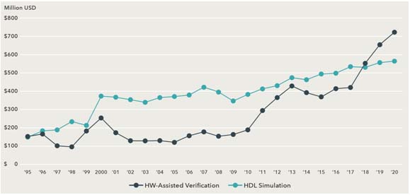
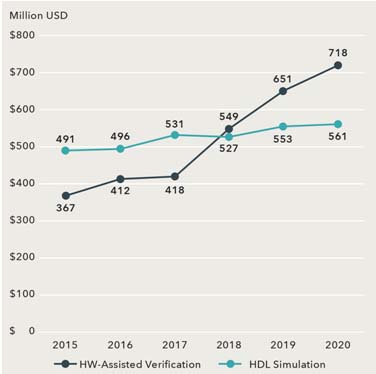
The prominent and, today, mandatory role played by hardware-assisted verification is captured in the annual revenue statistics published by the ESD Alliance, a SEMI Technology Community. In 2018, hardware-assisted verification revenues crossed over those of RTL simulation, and the trend continue. See figures 3a and 3b.
Hardware-Assisted Verification
Four key markets are driving hardware-assisted verification technology. They encompass networking, communications, specifically 5G, computing and storage, and transportation, not only automotive but any type of transportation where autonomous driving is possible.
All four key markets share a common theme: Software performance defines semiconductor success. They also share the same challenges, specifically power and performance analysis very early in the design flow to verify that the design specifications are met.
When hardware dominated chip design, verification was used to confirm that the hardware functional specifications were met and ensured no hardware bugs compromised design behavior. Today, meeting hardware functional specs is just the first step. As important is to verify that the DUT’s power and performance conform with target requirements. This can only be achieved by executing real-world workloads, frameworks, and a broad range of market-specific benchmarks. Finally, thorough SoC in-system validation has become necessary before releasing the DUT to manufacturing.
Industry Benchmarks
Accurate power and performance analysis can only be achieved by processing software benchmarks on RTL DUTs and they are unique to each vertical market segment. See figure 4.
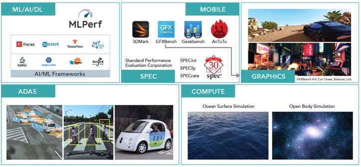
Examples of benchmarks in key industries:
- In artificial intelligence applications, including machine learning and deep learning, the most common benchmark is the MLPerf framework that includes a broad benchmark suite to measure performance of software frameworks.
- In advanced driver assistance systems (ADAS) applications, a sensor framework computes massive amounts of sensor and raw data fusion to formulate a decision to act upon.
- In the mobile market, AnTUTU has been the reference benchmark for many years.
- In graphics-heavy designs, a popular benchmark is GFXBench from Kishonti.
- In computing, a prevalent benchmark is ocean surface simulation, open body simulation based on very advanced computations.
- In HPC designs, widespread is SPEC (Standard Performance Evaluation Corporation) with SPECint, SPECfp and SPECrate, reference benchmarks for integer and floating-point units.
Workloads and Benchmarks Execution
Workloads and benchmarks execution demands a best-in-class hardware-assisted verification environment for three reasons.
- First, workloads and benchmarks consist of long software code sequences that require considerable numbers of verification cycles. This is compounded by the need to boot an OS that calls for billions of cycles.
- Second, accurate power and performance analysis demands full DUT visibility to capture power activity, as well as comprehensive debug tools to trace issues that may hinder performance.
- Third, the massive size and complexity of the DUT reaching into several billion gates in a single design.
Hardware-assisted verification is the only option to handle all three issues.
The Verification Process
Based on the long-standing principle that the cost of finding bugs increases by an order of magnitude at each subsequent verification step, the early verification activity concentrates on unearthing as many bugs as possible starting at the IP/hardware block level and bare-metal software.
As verification moves up the abstraction layers, the amount of uncovered design bugs decreases rapidly. The time to find them that is measured in number of verification cycles, however, increases dramatically. Hardware verification and software validation efforts progress in five stages on two complementary curves. Mapped on a timeline versus verification activity, the curves evolve in seven steps delimited by milestones, as shown in Figure 5.
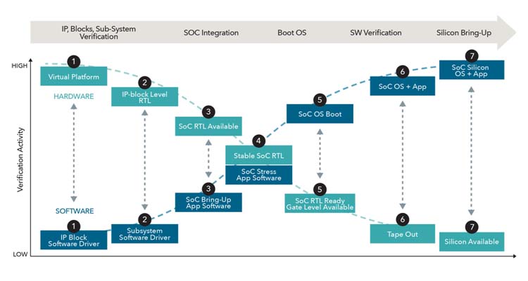
The flow begins with IP, block and subsystem verification then moves to SoC integration, OS booting and software verification, and it ends with silicon bring up.
From the hardware perspective, the seven milestones, shared by the majority of semiconductor companies, include:
- Virtual platforms
- IP block level RTL code
- Availability of SoC RTL code
- Stable SoC RTL code
- Completely debugged RTL code (at this point, the full SoC gate-level netlist is available)
- Backend implementation begins and proceeds with tape out
- First silicon delivered by manufacturing
In each step, specific design tasks are executed and accomplished by dedicated verification tools with unique characteristics appropriate for those tasks. See table 1.
| STAGE | HARDWARE VERIFICATION | SOFTWARE VERIFICATION | BEST TOOL |
| 1 | Architectural Validation | Bare-Metal validation | Virtual Platform |
| 2 | Block/IP RTL Verification | SW Driver Validation | RTL Simulation + Emulation |
| 3 | SoC RTL Available | OS Boot | Emulation |
| 4 | Stable SoC RTL | Full SW Stack Validation | Emulation + Prototyping |
| 5 | SoC RTL Ready (Gate level) | SW Workloads/Benchmark Testing | Prototyping + Emulation |
| 6 | Tape-Out | Full System Validation | Prototyping + Emulation |
| 7 | Silicon Availibility | Silicon Bring-Up | Prototyping + Emulation |
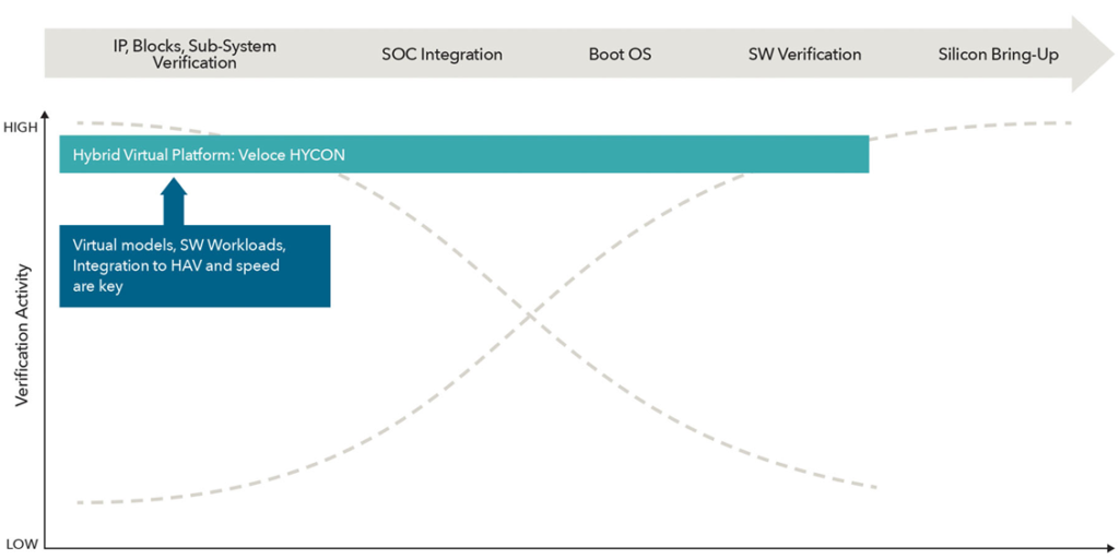
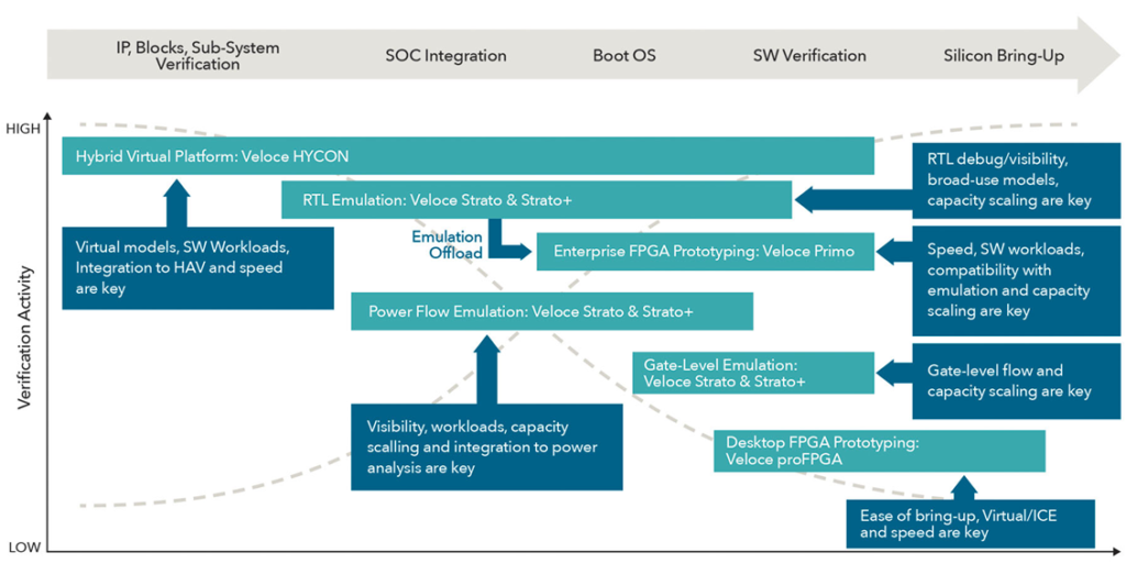
Step-by-Step Verification The verification flow begins with the deployment of a virtual platform. This requires three ingredients: a wide range of virtual models, robust software workloads and tight integration to a hardware-assisted verification platform to achieve a high speed of execution. A virtual platform like Veloce HYCON from Siemens EDA can be used from early software testing all the way to full software validation. See Figure 6
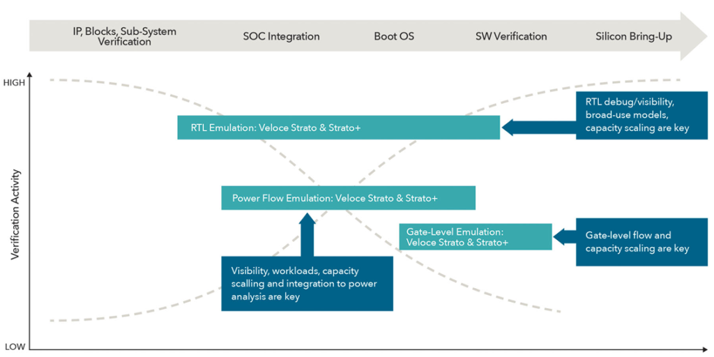
Next is IP/Block RTL verification. For this task, it is imperative to provide full RTL visibility. While this is available with RTL simulation, only RTL emulation can support verification of hardware with software. For RTL emulation, a fundamental requisite is support for scalable capacity to accommodate the full hierarchy of an SoC design from IP/block to subsystem block to a full SoC. Additional capabilities include workload scalable capacity and broad use of models.
When the design reaches a certain level of maturity, power and performance analysis can be undertaken. While internal design visibility is key, workload capacity scaling and integration with power analysis tool are necessary capabilities.
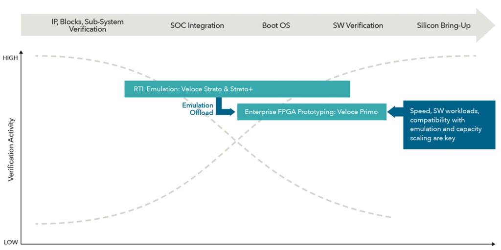
Moving closer to gate level and tape out, gate-level emulation is necessary. Siemens EDA’s Veloce Strato and Veloce Strato+ excel in this regard. See figure 7.
At this stage of the flow, the ability to debug the DUT can be traded off for higher speed. Fast execution is advantageous for booting an OS, validating application software, including benchmarks and workloads. Higher speed cannot be compromised with design capacity and compatibility with emulation is also a key capability. The best tool for the job is Siemens EDA’s Veloce Primo Enterprise FPGA Prototyping because of its faster speed, up to 10 times that of the emulator. Still, emulation is necessary for tracing bugs in hardware when they pop up during software validation. See figure 8.
DA)
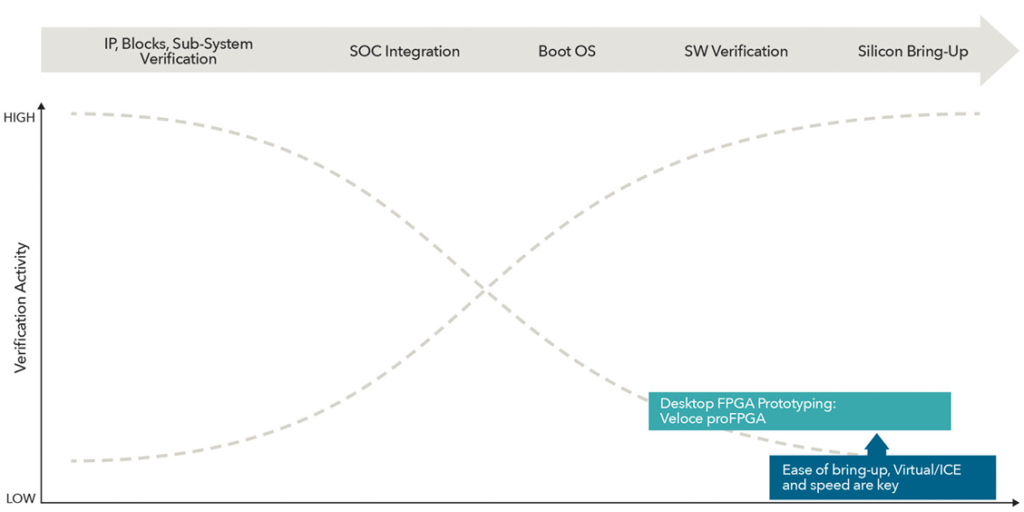
Complementary to an enterprise FPGA prototyping platform, a desktop FPGA prototype like Veloce proFPGA provides a lower footprint capacity and higher speed than the former. Targeted to software validation, ease of bring up and a complete range of use models from virtual to ICE are key. See figure 9.
THE CASE FOR AN INTEGRATED HARDWARE-ASSISTED VERIFICATION PLATFORM
Table 1 on page 45 shows that emulation is the best tool in all seven steps of the verification flow, and a must have platform for hardware-software integration. The combination of running fast enough for processing software and full design visibility for efficient debug makes it unique for the demanding task of booting an operating system and processing workloads on top of the target hardware to carry out accurate power and performance analysis.
FPGA Prototyping, however, is the preferred choice when design visibility is secondary to execution speed.
Essentially, both emulation and prototyping share four steps from step #4 to step #7 as best verification tools.
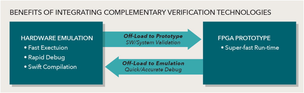
A significant boost in verification productivity can be achieved by tightly coupling a best-in-class emulation platform, like Veloce Strato+ with a state-of-the-art enterprise FPGA prototyping platform like Veloce Primo. The combination of emulation with prototype in virtual mode when the DUT is driven by a software-based test environment functionally equivalent to a physical test target. It enables verification engineers to quickly reach a point in time when a bug shows its effect using the prototype, stop and load the same DUT in emulation, and efficiently trace that bug using the emulator.
Instead of competing for the same verification job, emulation and prototyping can complement each other to accelerate the verification cycle and increase the quality of the DUT. See Figure 10.
CONCLUSIONS
Today, hardware emulators and FPGA prototypes have become mandatory verification platforms to thoroughly debug and validate an SoC design.
Emulators excel in hardware debug and hardware/software integration with quick design iterations made possible by fast compilation times and thorough design debug. They also allow for performance and power analysis driven by real-world workloads. Veloce Strato+ is an excellent choice for these tasks.
FPGA prototypes stand out in speed of execution by trading off design visibility. Veloce Primo offers unique capabilities for this task.
A tight integration between hardware emulation and FPGA prototypes lowers the cost-per-verification cycle, accelerates the time to identify verification issues, optimizes the utilization of both verification platforms, and, ultimately, boosts the return on investment.