
Build testability into a custom chip during the design phase
Source: Electronic Product

Of all the electronic design automation (EDA) tools on the market, design for test (DFT) may be the most under-appreciated; even though building testability into a chip during the design phase will significantly lower hefty testing costs. According to recent analysis, the cost of testing a batch of chips after manufacturing to determine which parts are free of manufacturing defects has reached an alarming threshold of 40% of the cost of building the chip.
DFT can eliminate the risk of passing a problem device that eventually will be caught in the field at a cost much higher than if found on the manufacturing floor. It may also avoid the rejection of faultless devices, thus increasing the yield. Inserting DFT also reduces the time associated with test development, as well as the execution time of testing fabricated chips.
DFT, an electronic industry catchphrase, goes with automatic test pattern generators (ATPG) and memory built-in-self-test (MBIST), and is the insertion of an on-chip test infrastructure, such as scan chain, MBIST structure, or compression/decompression logic. Scan chain adds controllability and observability through serial shift-registers. With scan chain, the problem of testing a circuit is simplified and reduced to testing the combinational logic between registers. The ability to automatically generate test patterns via ATPG tools can alleviate the time-consuming and tiresome task of creating test vectors.
The on-chip test infrastructure, or scan chain, is inserted at the gate-level netlist after the design has been functionally verified and caution must be exercised as it can interfere with the chip’s functional correctness. The design change requires gate-level verification to assure that the design integrity has not been compromised. The testing is performed by long sequences of test patterns, a compute-intensive task that is by far more onerous that register transfer level (RTL) verification.
It is worth mentioning that from the design viewpoint the creation and insertion of the DFT structures are rather simple. From the density and size perspective, however, the design gets rather large, and the volume of test patterns required to test the design significantly increases size.
DFT verification
Simulator-based verification is too slow for gate-level checks when design sizes are reaching into the hundreds of million gates. The DFT approach only makes things worse. If that wouldn’t be enough of a burden, priority access to a simulation farm approaching tape-out favors design engineers and plays against test engineers. Chips often are taped-out with minimal DFT verification, and thorough DFT testing is performed after tape-out, too late to fix design faults.
DFT verification comes in various forms, including custom initialization patterns that need to be verified. It could be an on chip clock controller inserted by an automatic test pattern generation tool that needs to be dynamically verified during pattern execution, or logic added for MBIST that requires functional verification of the associated logic with the test pattern. An SoC may include a custom initialization pattern that configures a test and causes a transition from a functional mode to a test mode. Other test modes may have low-power techniques where parts of the chip are put into a low-power mode during test, which requires validating the test infrastructure under appropriate conditions.
Hardware emulation with a DFT app
Hardware acceleration accelerates the simulation cycles required to do a thorough DFT verification. It can enable verification the chip functionality, regardless of its size and complexity.
While hardware emulation has been used for 30 years to increase verification cycles by deploying re-programmable hardware, new deployment modes are making it a far more viable verification tool and paved the way for an “apps” approach. Some recently announced apps for hardware emulation could be welcome news for those chip design teams using the more difficult simulator-based verification approach. The DFT app accelerates a chip design schedule that requires comprehensive gate-level simulations. Taking advantage of automatically generated patterns, the design team can shorten the overall pattern development cycle.
This type of hardware emulation’s scalable hardware and compiler enable test pattern validation for large gate-level designs, with scan and other test structures embedded into the design. Its high performance enables more simulation cycles, speeding DFT analysis. The DFT app is interoperable with other tools because it supports the industry-standard STIL format file used on the production tester to identify chips damaged during manufacturing.
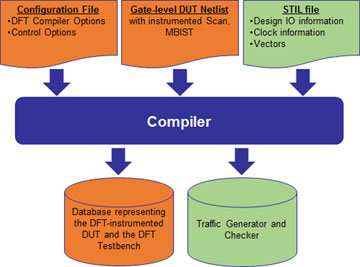
DFT apps for hardware emulation change the compilation flow and run-time execution in the deployment process of a hardware emulator. These are a change in the compilation flow and in the run-time execution. A gate-level design with scan and MBIST is fed into the hardware emulation’s compiler. The compiler creates the necessary testing infrastructure for reading test vectors from the STIL file, applying them to the synthesized device under test (DUT) and comparing outputs. The compiler re-compiles and synthesizes the user netlist into a structural description compatible with hardware emulation. At compile time, the emulator creates the necessary infrastructure for reading test vectors from the STIL file and applying them to the synthesized DUT, then re-compiles and synthesizes the netlist to a structural description compatible with emulation. The test harness includes a mechanism to compare the outputs. See figure #1.
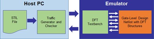
The design and testbench are mapped into the emulator when invocated. During runtime, hardware emulation pulls test vectors from the STIL file, applies them to the DUT, and compares the output — all at emulation speed. See figure #2.
DFT apps enable execution of complete pattern sets for DFT verification to shorten the pattern development cycle. A scalable emulation platform that can accommodate designs of up to a couple of billion gates together with a compiler that can support a DFT methodology empower test pattern validation for large gate-level designs with scan and other test structures embedded into them.
Once the chip has been manufactured, the same STIL file can be used on the testing floor. Loaded into an ATE, the test vectors exercise the chip and its responses get compared with the expected values in the STIL file.
Design for test
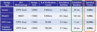
Hardware emulation does not simulate at incrementally better speeds than simulation – it is orders of magnitude faster. Some benchmarks show four or five orders of magnitude improvement when running DFT patterns on hardware emulation. See table #1.
By reducing tests that normally take three months long on a simulator to two hours, hardware emulation allows complete validation of test vectors and DFT logic before chip tape-out. Offering a DFT app for hardware emulation broadens the use model, improves performance and helps a verification engineer avoid risk. DFT engineers now have a way in which to utilize the horsepower of hardware emulation to ensure a chip is fit for manufacturing using an “app.”