
Source: Embedded Computing Design
Chip design debug is a difficult discipline, and system-on-chip (SoC) design has made it more so. It’s like the proverbial needle in the haystack. For SoC designs it’s two haystacks, one for software, the other hardware. Software development groups often point a collective finger at the hardware group claiming it’s a hardware bug, while the hardware group snaps back, claiming it is a software bug. It’s hard to know who’s right without effective verification tools to pinpoint the problem. That’s where hardware emulation comes in.
Hardware emulation can be invaluable for debugging hardware and for testing the integration of hardware and software within SoC designs well ahead of first silicon. When two disparate parts of the engineering group – hardware designers and software developers – use emulation, they’re able to share the same system and design representations. Combined software and hardware views of the SoC design enable them to work together to debug hardware and software interactions.
As the foundation of most SoC verification flows, hardware emulation allows engineering groups to plan more strategically and implement a debugging approach based on multiple abstraction levels. Engineering groups don’t have to dive into two haystacks independently of one another. Instead, they can track a bug across the boundary between the embedded software and the underlying hardware to determine whether the problem lies in the software or in the hardware.
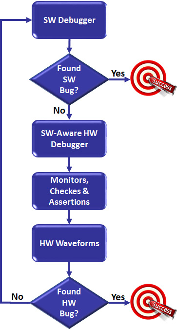
Implementing a debugging methodology based on multiple abstraction levels starts with embedded software at the highest level, and moves down in abstraction levels to trace the behavior of individual hardware elements. In fact, starting from a database comprising multi-billion clock cycles, a software debugger can localize a problem to within a few million clock cycles. At this level, either the software developers can identify the source in the software code or their hardware design counterparts can use a software-aware hardware debugging approach to focus on a lower level of abstraction. The methodology calls for monitors, checkers, and assertions implemented through hardware transactors that avoid speed degradation and help narrow down the problem to a few thousand cycles.
Once the collected data at those two levels has been reviewed, hardware emulation allows the engineering group to move down to the signal level. It can analyze the information via the register transfer level (RTL) waveforms of the identified period of time and trace its likely origin. Either a hardware bug is unearthed or the hardware is cleared of failure. If it’s the latter, it forces the decision to move back to the software environment.
Navigating multiple levels of debug abstraction
Navigating between different levels of abstraction – from software through hardware and back – avoids long simulation runs and wading through massive amounts of detailed data (Figure 1).
The multi-level debugging methodology would not be possible with software simulators because they are too slow to effectively execute embedded software. Indeed, they would run for many months to process billions of cycles on designs whose sizes reach into several hundreds of millions of application specific integrated circuit (ASIC) equivalent gates. This is an unacceptable time constraint for suppliers of consumer electronics devices, or any other electronics devices for that matter.
While still widely used, the in-circuit-emulation (ICE) mode, the original style of emulation that drove its success in the verification scene, now faces a viable alternative in transaction-based verification. Conceptually, the idea is simple. Tests are written at high levels of abstraction and the conversion from high-level commands to bit-level signals is moved from the testbench into a dedicated entity called a transactor. By mapping the transactor onto a hardware emulator, acceleration of five or six orders of magnitude compared to simulation-based verification can be easily achieved.
Engineering groups use transactors to build a virtual test environment instead of the ICE physical target system by replacing a set of I/O protocol-based speed adapters with an equivalent set of transactors (Figure 2).
Design debugging is simplified in transaction-based acceleration. By gaining full control of the design clocks that aren’t sourced by the hardware test bed, debugging becomes easier and more efficient. By controlling the clock frequency, it’s possible to stop the emulated design-under-test (DUT) model, read its memory content, force some registers, or dump the waveforms.
Traditionally, debugging in an ICE environment required hardware logic analyzers driven by the uncontrollable clocks coming from the target system. The setup caused nondeterministic behavior and compromised the ability to debug the DUT. Hardware emulation vendors recently addressed the random behavior of the ICE periphery with methods to convert it into a deterministic behavior.
A multi-level perspective of co-verification
Once software designers and hardware developers experience transaction-based verification using hardware emulation, their entire verification perspective changes. The ability to quickly setup a powerful test environment free of cumbersome ICE hardware means easier and more effective debugging. The goal may be the same – better designs in less time – but the experience now can be something far less challenging.
Engineering groups are finding that modern hardware emulators are a requisite to test the hardware and integrate hardware and software in SoC designs. It allows them to plan more strategically and to successfully implement hardware/software co-verification.