By Jean-Marie Brunet, and Dr. Lauro Rizzatti
Today, system-on-chip (SoC) devices permeate our world and propel numerous industries. They are integral for the internet of things (IoT), to power up complex 5G/6G wireless applications, sit at the core of artificial intelligence/machine learning (AI/ML) algorithmic processors, drive powerful data center computers and storage devices, and are at the heart of autonomous driving vehicles.
These devices share a common trait—the combination of hardware and software with varying complexity. In leading industries, the hardware at the top-end reaches several billion gates, hierarchically organized in structures that include a variety of CPUs, GPUs, custom cores and logic, memories and many peripherals. Conversely, the software content or workload extends over hundreds of millions or even billions of lines of code, allocated hierarchically, from bare-metal software to multiple operating systems, and an assortment of large applications.
Verification and validation of such designs is undertaken on a tight schedule and littered with challenges. Taming the challenges is imperative to deliver a properly functioning product on time and prevent profit losses with catastrophic financial consequences.
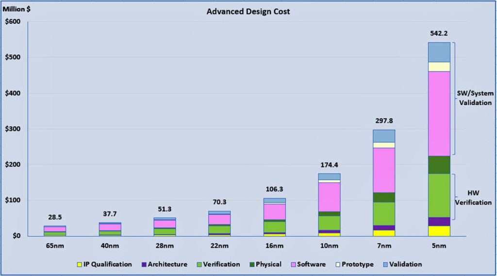
An indirect measure of the challenges is captured in figure 1 that charts cost for design complexity at sample process technology nodes. Performing verification and validation of hardware and software accounts for the largest effort. In 5-nanometer (nm) technology, that effort exceeds 70 percent of the entire design and verification cost.
Mandatory for accelerating the verification cycle and reducing the risk of missing a scheduled tape out, are hardware-assisted verification platforms that include hardware emulation, field programmable gate array (FPGA) prototyping and tools to validate software in the context of the end product.
Hardware-assisted verification/validation platforms
Hardware emulators and FPGA prototypes are not new technologies and have been around for decades. Broadly speaking, emulators offer design capacity, speed of execution and debug visibility necessary to debug the system-on-chip (SoC) hardware, including software drivers and operating systems. FPGA prototyping complements emulation by providing the additional speed required for processing large software workloads and for running long regression suites.
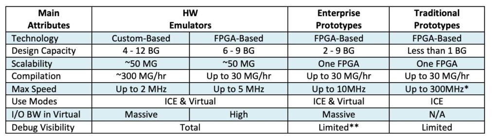
At a closer inspection, five main differences separate emulators from FPGA prototypes: design capacity/scalability, compilation speed, execution speed, design debug capabilities, and use models.
Best-in-class hardware emulators boast design capacity in the multi-billion ASIC-equivalent gates range with extensive scalability to support multiple concurrent users. They compile the design under test (DUT) at orders of magnitude faster than FPGA-based prototyping platforms. Their execution speed of a couple of megahertz coupled with massive input/output throughput support processing real-world workloads, including industry-specific frameworks and benchmarks. They provide design visibility, as well as bug tracing capabilities for quick and effective hardware debug. They can be deployed in in-circuit emulation (ICE) mode and in virtual mode. In ICE mode, the DUT is driven by the physical target system where it ultimately will reside driven by real-world traffic subject to random behavior. In virtual mode, the DUT is exercise via software models leading to a deterministic and repeatable environment. Repeatability is critical to perform low-power design analysis, evaluate power estimation by keeping track of DUT internal activity, and assess overall design performance before silicon availability. Deployment in virtual mode supports remote access 24/7 from anywhere in the world.
Traditional FPGA prototypes are resources deployed in ICE mode. With design capacity of less than one-billion gates, they trade off usage flexibility, hardware debug capabilities and quick compilation for two orders of magnitude faster execution speed than hardware emulation on the same design size at a fraction of its cost.
In that past couple of years, enterprise prototyping has been bridging the gap between emulation and traditional FPGA prototyping. In combination with emulation, the enterprise prototype increases the productivity of verification teams. By sharing several characteristics with the emulator, such as large capacity, extensive scalability, multi-users, and virtual deployment, the enterprise FPGA prototype can replace the emulator on-the-fly and provide the best attributes at each stage of the verification flow.
Table I shows the main attributes of the three hardware verification engines.
Software-enabled verification/validation methodology
As shown in Figure 1, for a number of years, the cost to validate software has been offsetting the cost to verify hardware, and the disparity continues to diverge. This reality has forced a revaluation of the verification/validation methodology favoring the software component. Software and full-system validation is now a critical factor –– the sooner it is carried out, the faster the entire verification cycle can be completed with better testing and lower risk of missing the schedule.
One recent approach from the electronic design automation (EDA) industry consists of virtualizing the SoC design into a model using a high-level abstraction language before register transfer level (RTL) code is available and stimulating that model with real-world software workloads. Software workloads comprise industry specific frameworks, benchmarks and applications. Benchmark examples in key industries include: MLPerf in artificial intelligence and machine learning (AI/ML) applications; AnTUTU, Geekbench, and GFXBench in the mobile market; Car Chase and Manhattan in graphics-heavy designs.
As RTL code becomes available, the high-level models of the SoC combine with available RTL code until the entire SoC model achieves full RTL status. Since processing real-world workloads demands execution of hundreds of billions of verification cycles, the RTL code can only be handled by hardware-assisted verification platforms, namely, emulators and FPGA prototypes.
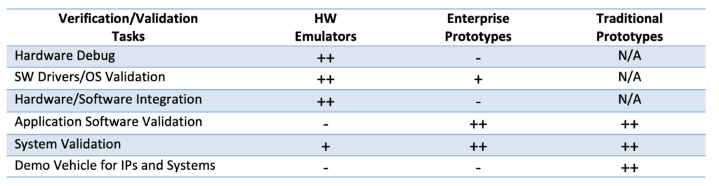
Table II highlights the best fit for each hardware-assisted verification tool.
The “Shift-Left” verification/validation methodology
By deploying all verification tools in parallel and taking advantage of their best characteristics, it is possible to move software validation upstream concurrently with hardware verification, and, in the process, shrink the time to tape out. This is a “shift-left” methodology.
Early in the design cycle, emulators verify subsystems prior to assembling a complete SoC design, while hardware description language (HDL) simulators tackle intellectual property (IP) blocks and smaller design blocks. As early RTL code becomes available, emulators validate bare-metal software and drivers. Later in the design cycle, when full SoC RTL code reaches stability, emulators validate operating systems and the entire hardware system by executing real-world workloads.
Fast compilation and full design visibility of emulators accelerate “compile-run-debug” iterations, supporting multiple iterations per day even on the most complex SoC designs. By providing full hardware and software debugging capabilities to both hardware and software engineering teams, development groups collaborate and debug integration issues in a way that was not possible before.
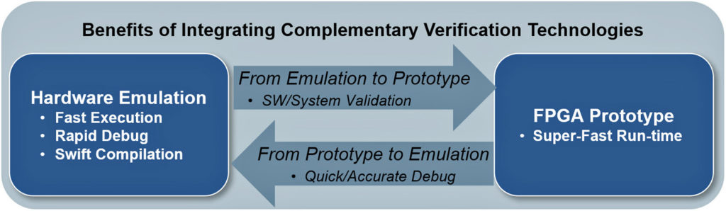
A caveat is the slower execution speed of emulators vis-à-vis FPGA prototypes that puts emulators in a secondary role for application software validation. Combining the two in a unified flow exploits the strengths of each leading to a powerful verification/validation environment for effective and faster design verification.
For instance, after performing hardware debug via emulation, the DUT is moved to an FPGA prototype to accelerate applications software validation, freeing the emulator to carry out power and performance analysis. If a design bug shows up during software testing, the design can be moved back to the emulator for bug tracing quickly and efficiently (Figure 2).