
Source: ChipDesign
Several years ago, while at Automatic Test Equipment (ATE) leader Teradyne, I witnessed frequent debates on a fundamental dilemma: On the production/testing floor, is it better to pass a failing device or reject a good device? Obviously, both are bad choices. If you reject a good device, you shoot yourself in the foot since you lower the yield of your manufacturing facility and take a hit on profits. But if you pass a failing device, the undetected manufacturing flaw will eventually be found in the field at a cost several times higher than on the manufacturing floor, impacting profits and, worse, your reputation with customers.
The above is still true today; it just got worse. Recent statistics reveal that the cost of testing a batch of chips after manufacturing to determine which parts are free of manufacturing defects (as opposed to free from design bugs), adds up to 40% to the cost of building the chip.
The above considerations drove the electronics industry to devise methods to build testability into the chip at the design stage aimed at lowering the testing costs. Called Design for Testability (DFT), it made it possible to:
- Assure the detection of all faults in a circuit
- Reduce the cost and time associated with test development
- Reduce the execution time of testing fabricated chips
Broadly speaking, over time, the industry devised two forms of DFT: ad-hoc and structured.
Ad-hoc DFT consists of a set of rules to promote “good” design practices to ease and accelerate the testing process. Examples include making all flip-flops initializable by providing set and reset signals, avoiding asynchronous logic feedbacks that can result in oscillation, eschewing gates with a large fan-in since they make the inputs difficult to observe and outputs difficult to control. Or, provide test control for difficult-to-control signals. For example, signals produced by a long counter require many clock cycles to control, which increases the length of the test sequence. Generally speaking, ad-hoc DFT does not add logic, i.e., does not consume silicon in the design.
Structured DFT: Scan and BIST
Structured DFT involves adding extra logic for test according to some procedure. The most commonly used structured methods are Scan and Built-In-Self-Test (BIST).
Scan was first mentioned in 1973 by Williams and Angell. Sequential circuits –– as opposed to combinational designs –– are difficult to test. The main idea behind scan was to make the internal memory elements part of a shifter register chain to provide controllability and observability through serial shifts. With scan chain, the problem of testing any circuit is reduced to testing the combinational logic between registers. The basics are to convert each flip-flop to a scan register. The only cost is one extra multiplexer. In normal mode, flip-flops behave as usual. In scan mode, they behave as shift register. The contents of flops can be scanned out and new values scanned in. More to the point, the method allowed the development of automatic test pattern generators (ATPG), and alleviated the time-consuming and tedious task of creating test vectors.
As circuit complexity increased over time, VLSI design in the 90s and in the new millennium of SoC chips, tester costs surged dramatically as did the cost of test program development. Just consider:
- Extremely high and still increasing logic-to-pin ratio on the chip makes harder to accurately control and observe the inner workings of the device, essential for testing
- SoC devices are increasingly dense and faster with each drop in process technology node
- Test pattern generation and application are getting extremely long
- Prohibitive amounts of test data must be stored in the ATE
- Increasingly difficult and horrendously expensive to perform at-speed testing (at GHz)
- Unfamiliarity with gate-level structures of the design-under-test (DUT), since logic is now automatically synthesized from hardware description languages (HDLs), thus compounding the problem of testability insertion.
- Dramatic lack of skilled test engineers
To cope with this unstoppable trend, the industry responded by integrating some tester capabilities onto the chip, hence the name BIST. BIST reduced the complexity and, thereby, decreased the cost and reliance upon external (pattern-programmed) test equipment in two ways:
- Decreased test-cycle duration
- Eased the complexity of the test/probe setup by shrinking the number of I/O signals that must be driven/examined under tester control.
Further, it made it possible to test circuits at speed (at GHZ), leading to more thorough examination.
The basic approach was to compress “good” test responses into a “signature” and implement pseudo-random (or pseudo-exhaustive) pattern generators (PRG) onto the chip. BIST is indeed the integration of pattern generation and response evaluation on chip.
In the most popular BIST methodology, scan cells are modified to generate pseudorandom test vectors at the input to a logic block, and then to collect a signature at the output (using a linear feedback shift register). Examples of BIST include LFSR (Linear Feedback Shift Register) used to generate pseudo-random sequence, and MISR (Multiple Signature Input Register) used to generate signature of tested circuit.
BIST consumes more silicon area and more verification cycles (as pseudorandom), but saves on the cost of generating and storing test vectors. Also, BIST often takes less elapsed time as it can often be run at full clock rate.
DFT Verification
Scan and BIST usually are incorporated in the design after it has been verified to be functionally correct. Unfortunately, the insertion of the on-chip test infrastructure, i.e., scan chain, BIST structure and compression/decompression logic, may interfere with its functional correctness. It is essential to perform a gate-level verification of the design after the DFT implant.
Off the bat, HDL simulation cannot do the job. Given the level of design complexity, gate-level simulation would require many months –– let’s make it years –– for a thorough, complete verification.
This task is a perfect match for a hardware emulation platform.
Emulation with a DFT App
Mentor Graphics recently announced a DFT “App” for hardware emulation that includes all that is needed to achieve the objective.
Its compiler creates the necessary testing infrastructure for reading test vectors from the STIL file, applying them to the synthesized DUT, and for comparing the outputs. The compiler also re-compiles and synthesizes the user netlist into a structural description compatible with emulation. See figure 1.
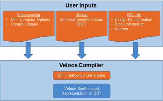
With a DFT App, user inputs are fed into the hardware emulation’s compiler. The emulator synthesizes a representation of the DUT. Source: Mentor Graphics
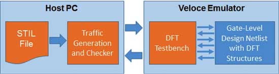
During runtime, the Veloce Emulation Platform fetches test vectors from the STIL file, applies them to the DUT, and compares the output at emulation speed. Source: Mentor Graphics
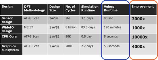
Emulation performs at orders of magnitude faster speed than simulation, which the table summarizes with DFT App benchmarks, showing four or five orders of magnitude improvement when running DFT patterns. In practical terms, three-months worth of simulation can be accomplished in a couple of hours in emulation. Source: Mentor Graphics:
Conclusion
A DFT App enables execution of complete pattern sets for DFT verification in a reasonable time to shorten the pattern development cycle. Scalable hardware and a compiler enables test pattern validation for large gate-level designs with scan and other test structures embedded into the design. The DFT App is interoperable with other tools by supporting standard STIL format file.
An emulation session provides enough verification power to pull the DFT schedule within the time the project management has scheduled, thus accelerating the time to market, increasing the yield, and ultimately augmenting profits.
About Lauro Rizzatti
Dr. Lauro Rizzatti is a verification consultant and industry expert on hardware emulation. Previously, Dr. Rizzatti held positions in management, product marketing, technical marketing, and engineering.