
Design capacity in hardware emulators, also the compilation flow, is heavily dependent on the type of technology used in the verification engine.
Source: EETimes

In my last blog post, I described differences in the maximum design capacity of a software simulator versus that of a hardware emulator, highlighting that not all emulators are created equal.
In this post, I focus on the compilation process in hardware emulators. Likewise, the design capacity in hardware emulators, also the compilation flow, is heavily dependent on the type of technology used in the verification engine. At this time, each of the three hardware emulation vendors has embraced its own architecture:
- Cadence: Processor-based architecture
- Mentor: Custom-FPGA-based or emulator-on-chip architecture
- Synopsys: Commercial FPGA-based architecture
The first two are based on custom chips; the third is built using arrays of commercial FPGAs. The compilation process is different, and unique to each architecture.
Let’s briefly recall the basics of a software compiler. A software compiler is a computer program or, better, a set of programs that transforms source code written in a programming language into an executable program made up of a sequence of instructions in the form of object code. The main operations performed by a compiler include lexical analysis, syntax analysis, semantic analysis, code optimization and code generation.
Compilation in software simulators
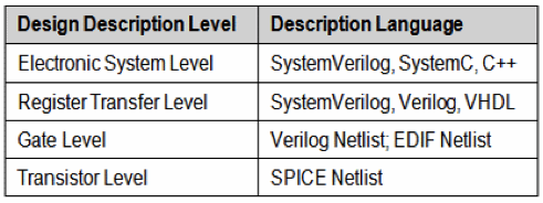
A simulator is essentially a software algorithm running on a computer. The algorithm processes data representing a design model described in a design language at one of multiple hierarchical levels as illustrated in Table 1.
The compiler converts the design model into that data structure, following the guidelines of a software compiler, with some differences.
Hardware compilation
When the output of a compiler targets computer hardware at a very low level, for example, an FPGA or a structured ASIC, it is a hardware compiler because the source code produced effectively controls the final configuration of the hardware and its operations. The output of the compiler is not a sequence of instructions. Rather, it is an interconnection of transistors or lookup tables. A quintessential example is the compiler of a hardware emulator.
Compiler in processor-based emulators
The operation of a processor-based emulator vaguely resembles that of a software simulator. In both engines, the design-under-test (DUT) model is converted in a data structure stored in memory. In the case of the emulator, the design data structure is processed by a computing engine implemented in a vast array of Boolean processors, which gives the name to the emulator type.
[Is FPGA better for vision applications? See how it compares.]
Typically, the vast array is made up by relatively simple 4-input ALUs, possibly reaching into the millions in fully expanded configurations. These processors are tasked with evaluating all logic (Boolean) functions in the DUT in a time order controlled by a sequencer.
The principle of the operation is exemplified in the following figure 1 and table II using an oversimplified approach.
All operations are scheduled in time steps and assigned to the processors according to a set of rules to preserve the functional integrity of the DUT.
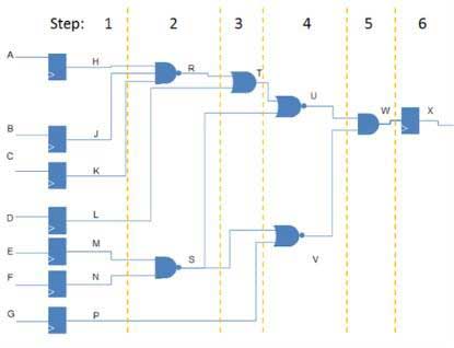
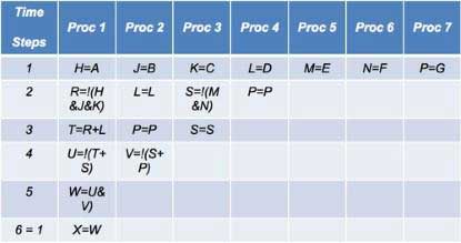
An emulation cycle consists of running all the processor steps for a complete execution of the design. Large designs typically require hundreds of steps. The more operations can be carried out in each step, the faster the emulation speed.
During each time step, each processor is capable of performing any input logic function using as inputs results of any prior calculation of any of the processors and any design input or memory contents. The more processors are available in the emulator, the more parallelism can be achieved with benefit for faster emulation time.
The compiler task consists of partitioning a design among the processors and scheduling individual Boolean operations in the time steps. The following are the main stages of the compilation flow:
- 1) Map RTL code into primitive cells such as gates and registers
- 2) Reduce Boolean logic (gates) into input functions
- 3) Assign all design inputs and outputs to processors
- 4) Assign each cell in the design to a processor
- 5) Schedule each processor’s activity into sequential time steps
The compiler optimizes the processor scheduling for any given configuration of the emulator to maximize speed and capacity. It also has to consider several additional issues, such as tri-state bus modeling, memory modeling, debug probing, triggering and other factors. The main tasks listed above, however, characterize the flow for a processor-based emulator.
What the compiler doesn’t have to deal with is the internal timing in FPGA emulators, one of the most critical issues in these emulators. Controlling timing in an array of FPGAs is hard, unpredictable, and a path to failure, unless attention and engineering talent is involved in designing the compiler.
For this reason processor-based emulation compiles much faster and with fewer resources. The compiler maintains all originally designated RTL net names for use in debugging in spite of the Boolean optimization it performs. This allows users to debug with signal names with which they are familiar.
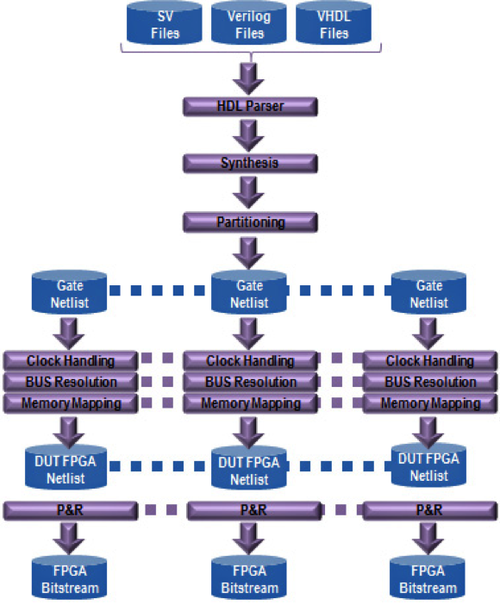
Compiler in FPGA-based emulators
The compiler of an FPGA-based emulator, whether based on custom or commercial FPGAs, is rather different than that of the processor-based emulator. It is more complex and includes additional stages not required in its counterpart. Differences between the custom versus commercial FPGA-based emulators concern some of the stages but not the overall flow, as highlighted later.
A compiler’s main tasks include RTL parsing, synthesis, netlist partitioning, timing analysis, clock mapping, memory mapping, board routing and FPGA placing and routing. The goal is to map the SoC RTL into a timing-correct, fully placed and routed system of tens or even hundreds of FPGAs.
Similarities with the processor-based emulator end with the mapping of the RTL code into a netlist of gates and registers.
Once the design has been synthesized, the netlist is partitioned across an array of FPGAs to implement the DUT. This is a critical step since assigning uneven blocks of logic to one or a few FPGAs may cause a sharp increase in interconnectivity that requires pin multiplexing at factors of 16x or 32x or possibly even higher. The impact on the emulation speed then can be deleterious.
Likewise, a partitioner that does not take timing into consideration may introduce long critical paths on combinational signals by routing them through multiple FPGAs, generating hops detrimental to the speed of emulation. An effective partitioner ought to include an accurate timing analysis tool to identify such long critical paths and avoid those hops.
The need to map clocks efficiently raises an even greater challenge. Modern designs can use hundreds of thousands of derived clocks distributed over hundreds of FPGAs. Designers reduce power consumption by using complex clock-gating strategies. A significant amount of effort goes into the compiler’s ability to manage these clocks well.
Finally, the FPGAs must be placed-and-routed.
Additional tasks, as for the processor-based emulator, are carried out by the compiler, but they are outside the scope of this article.
The compiler for an FPGA-based emulator requires leading-edge synthesis, partitioning, timing analysis, clock mapping, and place-and-route technologies.
What, then, are the differences in the compilation flow between a custom FPGA-based emulator and a commercial FPGA-based emulator?
I’ve written about architectural differences between the two approaches. Let me mention that in the custom FPGA used by Mentor Graphics in its Veloce2 emulator-on-chip platform, the interconnection network of programmable elements internal to the FPGAs and between FPGAs follows a patented architecture that secures predictable, repeatable, fast and congestion-free routing. It removes placement constraints and ensures simple routing and fast compilation. Clock trees are wired on dedicated paths independent from datapaths, leading to predictable and repeatable timing as well as the prevention of timing violations by construction because datapaths are longer than clock paths. Unpredictable timing and hold timing violations mar the viability of commercial FPGAs.
The architecture of the custom FPGA used in the emulator-on-chip ensures a high level of utilization of the reprogrammable resources. It is designed to ease the process of partitioning a large design into a large array of such custom FPGAs, and it allows for fast P&R. One spec says it all: Placing and routing one custom FPGA takes about five minutes, not far from 100X faster than P&R a leading commercial FPGA. It is not meant to be used as a general-purpose FPGA, however, since the capacity of the custom FPGA is lower than that offered by the largest commercial FPGAs.
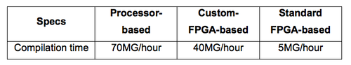
Table 2 compares compilation times among the three main types of emulation platforms.
Compiling a design is a time-consuming process, rather dependent on the design size and complexity. In an attempt to speed up the task, the process is heavily parallelized in multiple threads that can run concurrently on farms of PCs. This parallelization adds another dimension to the already difficult task of designing a compiler (Fig. 2).
In summary, all three types of hardware emulators present their own set of challenges to the hardware compiler. The compiler of the processor-based emulator is simpler and executes at faster speed vis-à-vis the FPGA-based emulators. Because of its architecture, the compiler of the custom-FPGA-based emulator avoids most of the traps of the commercial FPGA-based counterpart at a speed of compilation that is not far from the fastest processor-based emulator.